- 您现在的位置:买卖IC网 > Sheet目录342 > MCBSTM32EXL (Keil)BOARD EVALUATION FOR STM32F103ZE
�� �
�
�Advanced-control� timers� (TIM1&TIM8)�
�RM0008�
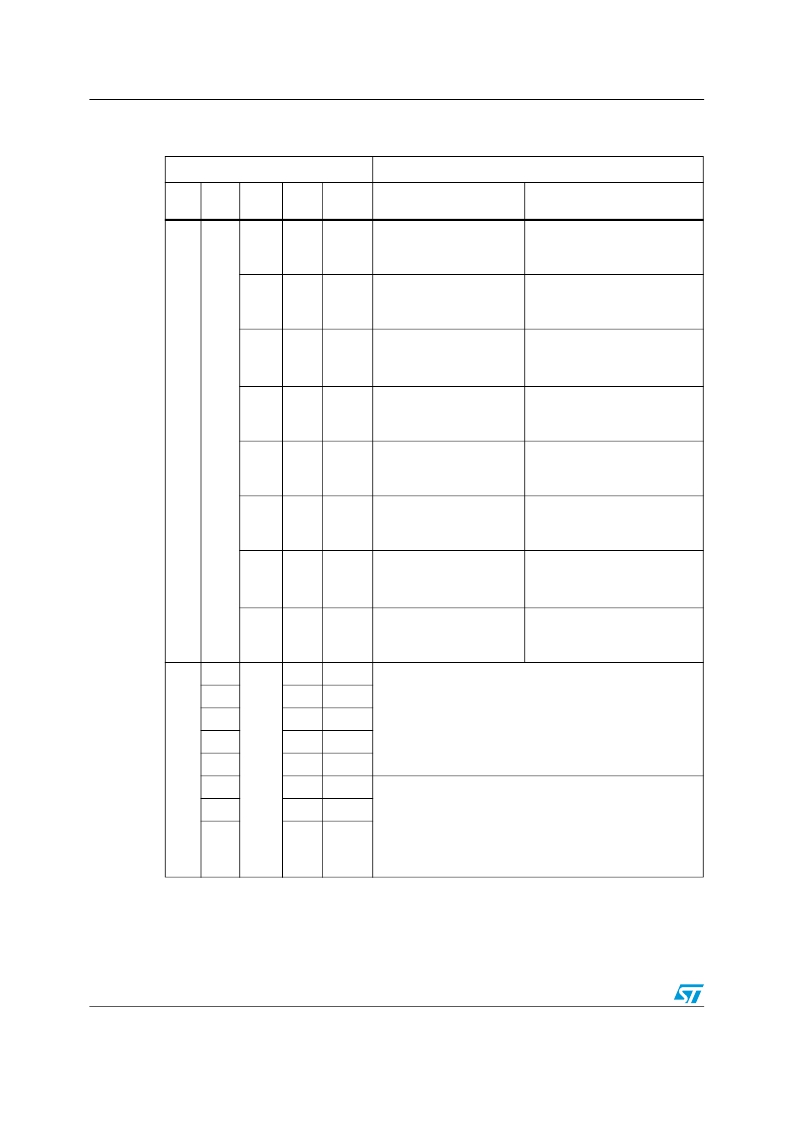
�Table� 73.�
�Output� control� bits� for� complementary� OCx� and� OCxN� channels� with�
�break� feature�
�Control� bits�
�Output� states� (1)�
�MOE� OSSI� OSSR� CCxE� CCxNE�
�bit� bit� bit� bit� bit�
�OCx� output� state�
�Output� Disabled� (not�
�OCxN� output� state�
�Output� Disabled� (not� driven� by�
�0�
�0�
�0�
�driven� by� the� timer)�
�the� timer)�
�OCx=0,� OCx_EN=0�
�Output� Disabled� (not�
�OCxN=0,� OCxN_EN=0�
�OCxREF� +� Polarity�
�0�
�0�
�1�
�driven� by� the� timer)�
�OCxN=OCxREF� xor� CCxNP,�
�OCx=0,� OCx_EN=0�
�OCxREF� +� Polarity�
�OCxN_EN=1�
�Output� Disabled� (not� driven� by�
�0�
�1�
�0�
�OCx=OCxREF� xor� CCxP,�
�the� timer)�
�OCx_EN=1�
�OCREF� +� Polarity� +� dead-�
�OCxN=0,� OCxN_EN=0�
�Complementary� to� OCREF� (not�
�0�
�1�
�1�
�time�
�OCREF)� +� Polarity� +� dead-time�
�OCx_EN=1�
�OCxN_EN=1�
�1�
�X�
�Output� Disabled� (not�
�Output� Disabled� (not� driven� by�
�1�
�0�
�0�
�driven� by� the� timer)�
�the� timer)�
�OCx=CCxP,� OCx_EN=0�
�Off-State� (output� enabled�
�OCxN=CCxNP,� OCxN_EN=0�
�OCxREF� +� Polarity�
�1�
�0�
�1�
�with� inactive� state)�
�OCxN=OCxREF� xor� CCxNP,�
�OCx=CCxP,� OCx_EN=1�
�OCxREF� +� Polarity�
�OCxN_EN=1�
�Off-State� (output� enabled� with�
�1�
�1�
�0�
�OCx=OCxREF� xor� CCxP,�
�inactive� state)�
�OCx_EN=1�
�OCREF� +� Polarity� +� dead-�
�OCxN=CCxNP,� OCxN_EN=1�
�Complementary� to� OCREF� (not�
�1�
�1�
�1�
�time�
�OCREF)� +� Polarity� +� dead-time�
�OCx_EN=1�
�OCxN_EN=1�
�0�
�0�
�0�
�0�
�0�
�0�
�1�
�1�
�0�
�1�
�0�
�1�
�Output� Disabled� (not� driven� by� the� timer)�
�Asynchronously:� OCx=CCxP,� OCx_EN=0,� OCxN=CCxNP,�
�OCxN_EN=0�
�Then� if� the� clock� is� present:� OCx=OISx� and� OCxN=OISxN�
�after� a� dead-time,� assuming� that� OISx� and� OISxN� do� not�
�0�
�1�
�1�
�1�
�X�
�0�
�0�
�1�
�0�
�1�
�0�
�correspond� to� OCX� and� OCxN� both� in� active� state.�
�Off-State� (output� enabled� with� inactive� state)�
�Asynchronously:� OCx=CCxP,� OCx_EN=1,� OCxN=CCxNP,�
�OCxN_EN=1�
�Then� if� the� clock� is� present:� OCx=OISx� and� OCxN=OISxN�
�1�
�1�
�1�
�after� a� dead-time,� assuming� that� OISx� and� OISxN� do� not�
�correspond� to� OCX� and� OCxN� both� in� active� state�
�1.� When� both� outputs� of� a� channel� are� not� used� (CCxE� =� CCxNE� =� 0),� the� OISx,� OISxN,� CCxP� and� CCxNP�
�bits� must� be� kept� cleared.�
�Note:�
�310/995�
�The� state� of� the� external� I/O� pins� connected� to� the� complementary� OCx� and� OCxN�
�channels� depends� on� the� OCx� and� OCxN� channel� state� and� the� GPIO� and� AFIO� registers.�
�Doc� ID� 13902� Rev� 9�
�发布紧急采购,3分钟左右您将得到回复。
相关PDF资料
MCBTMPM330
BOARD EVAL TOSHIBA TMPM330 SER
MCIMX25WPDKJ
KIT DEVELOPMENT WINCE IMX25
MCIMX53-START-R
KIT DEVELOPMENT I.MX53
MCM69C432TQ20
IC CAM 1MB 50MHZ 100LQFP
MCP1401T-E/OT
IC MOSFET DRVR INV 500MA SOT23-5
MCP1403T-E/MF
IC MOSFET DRIVER 4.5A DUAL 8DFN
MCP1406-E/SN
IC MOSFET DVR 6A 8SOIC
MCP14628T-E/MF
IC MOSFET DVR 2A SYNC BUCK 8-DFN
相关代理商/技术参数
MCBSTM32EXLU
功能描述:开发板和工具包 - ARM EVAL BOARD + ULINK2 FOR STM32F103ZG
RoHS:否 制造商:Arduino 产品:Development Boards 工具用于评估:ATSAM3X8EA-AU 核心:ARM Cortex M3 接口类型:DAC, ICSP, JTAG, UART, USB 工作电源电压:3.3 V
MCBSTM32EXLU-ED
制造商:ARM Ltd 功能描述:KEIL STM STM32EXL EVAL BOARD
MCBSTM32EXLUME
功能描述:开发板和工具包 - ARM EVAL BOARD + ULINKME FOR STM32F103ZG
RoHS:否 制造商:Arduino 产品:Development Boards 工具用于评估:ATSAM3X8EA-AU 核心:ARM Cortex M3 接口类型:DAC, ICSP, JTAG, UART, USB 工作电源电压:3.3 V
MCBSTM32F200
功能描述:开发板和工具包 - ARM EVAL BOARD FOR STM STM32F207IG
RoHS:否 制造商:Arduino 产品:Development Boards 工具用于评估:ATSAM3X8EA-AU 核心:ARM Cortex M3 接口类型:DAC, ICSP, JTAG, UART, USB 工作电源电压:3.3 V
MCBSTM32F200U
功能描述:开发板和工具包 - ARM EVAL BOARD FOR STM STM32F207IG + ULINK2
RoHS:否 制造商:Arduino 产品:Development Boards 工具用于评估:ATSAM3X8EA-AU 核心:ARM Cortex M3 接口类型:DAC, ICSP, JTAG, UART, USB 工作电源电压:3.3 V
MCBSTM32F200UME
功能描述:开发板和工具包 - ARM EVAL BOARD FOR STM STM32F207IG ULINK-ME
RoHS:否 制造商:Arduino 产品:Development Boards 工具用于评估:ATSAM3X8EA-AU 核心:ARM Cortex M3 接口类型:DAC, ICSP, JTAG, UART, USB 工作电源电压:3.3 V
MCBSTM32F200UME-ED
制造商:ARM Ltd 功能描述:KEIL STM32F207IG EVAL BOARD
MCBSTM32F400
功能描述:开发板和工具包 - ARM EVAL BOARD FOR STM STM32F407IG
RoHS:否 制造商:Arduino 产品:Development Boards 工具用于评估:ATSAM3X8EA-AU 核心:ARM Cortex M3 接口类型:DAC, ICSP, JTAG, UART, USB 工作电源电压:3.3 V